• 통큰쿠폰이벤트-통합
  • 통합검색(149)
  • 리포트(112)
  • 논문(30)
  • 시험자료(5)
  • 서식(1)
  • 자기소개서(1)

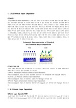
"atomic layer deposition." 검색결과 81-100 / 149건

  • 다양한 리소그래피법을 이용한 나노구조 형성
    Francesc Perez- Murano * Study of SU-8 conductivity: a) AFM topography image of the metallic electrodes deposited ... by nanostencil lithography on top of a very thin SU-8 layer. ... Vol. 283, 1999 NanoInk 사 홈페이지 (http://www.nanoink-inc.com)9 Conductivity of SU-8 Thin films through Atomic
    리포트 | 12페이지 | 1,500원 | 등록일 2013.06.17
  • Amino acid on Graphene
    This final shape enables proteins to accompl deposition Annealing 353-398K(5-10min) L- Cysteine Home ... SchematicGraphene LEED Data Graphene LEED Data (reference) Temperature dependent structural changes of graphene layers ... amino group carboxyl group α - carbon carboxyl carbon side chain(R group) hydrogen atom IntroductionGeneral
    리포트 | 31페이지 | 1,000원 | 등록일 2013.12.04
  • Si 기판에서 원자층 화학 기상 증착법으로 제조된 Al2O3 및 ZrO2 유전 박막의 결정학적 특성 및 계면 구조 평가
    한국재료학회 김중정, 양준모, 임관용, 조흥재, 김원, 박주철, 이순영, 김정선, 김근홍, 박대규
    논문 | 6페이지 | 4,000원 | 등록일 2016.04.02 | 수정일 2023.04.05
  • In-Situ doping during ZnO Atomic _badtags Deposition
    In-Situ doping during ZnO Atomic Layer Deposition Thin Film Mater Lab Journal of the Korean Physical ... layer deposition at 200˚C and evaluated the electrical and the optical properties of these films. ... July 2008, pp. 253-257Abstract Thin Film Mater Lab Al-doped ZnO films on glass and Si substrate by atomic
    리포트 | 11페이지 | 1,000원 | 등록일 2011.06.08
  • 각종증착장비에대하여...
    전력에 의한 PlasmAtomic Layer Deposition이란? ... CVD(Chemical Vapor Deposition)◎CVD란? ... CVD(Chemical Vapor Deposition)는 가장 널리 쓰이는 증착 방법으로 증착될 물질의 원자를 포함하고 있는 기체상태의 화합물을 이 기체가 반응을 일으킬 수 있는 환경을
    리포트 | 5페이지 | 1,000원 | 등록일 2010.04.13
  • [실험자료]원자층 단위 증착(ALD) 공정의 기본 원리
    Layer Deposition)1) 개 요ALD 기술은 CVD 기술과 달리 반응 원료를 각각 분리하여 공급하는 방식으로 한 cycle 증착 시에 표면 반응에 의해 1ML(monolayer ... 반응 화학물이 Wafer 위에 가지런히 증착되고, 나머지 불필요한 화학 반응 생성물은 Gas 상태로 만들어져 배기관을 타고 배출되는 구조를 나타낸다.▲ 원자층 증착장치(ALD: Atomic ... 이 론▲ 화학기상증착(CVD:Chemical Vapor Deposition)공정1) 개 요반응가스간의 화학반응으로 형성된 입자들을 웨이퍼표면에 증착하여, 절연막이나 전도성 막을 형성시키는
    리포트 | 6페이지 | 1,000원 | 등록일 2006.05.07
  • 박막증착 공정과 식각 공정 자료입니다.
    )EvaporationThe metal layers for all of the early semiconductor technologies were deposited by evaporation ... As the lateral dimensions of transistors have decreased, the thickness of many of the layers has remained ... To collect as many of these ejected atoms as possible, the cathode and anode in a simple sputtering system
    리포트 | 10페이지 | 1,000원 | 등록일 2010.06.23
  • 반도체제작공정-박막증착공정
    Metal deposition Pattern metal Etch metal Passivation layer deposition Open bonding pads{nameOfApplication ... longer same as those of bulkExistence of surface energy statesDifferent crystal structureDifferent inter-atomic ... gas in filmhigh vacuum path few collisions line of sight deposition little gas in filmhigher energy
    리포트 | 25페이지 | 2,000원 | 등록일 2010.09.09
  • DRAM에 관한 레포트입니다.
    박막공정 – ALD (Atomic Layer Deposition)ALD Process4. ... 박막공정 – ALD (Atomic Layer Deposition)● 낮은 온도에서 우수한 단차피복성과 균일한 조성을 가지는 박막을 형성 ● 박막 내의 불순물 농도를 감소 ● 반도체 ... 박막공정 – CVD (Chemical Vapor Deposition)4.
    리포트 | 18페이지 | 1,000원 | 등록일 2009.11.12
  • 반도체 제조 공정의 종류와 기법 서술
    .㉥ ALD(Atomic Layer Deposition) : 씨브이디와 유사하지만 반응을 원자층 단위로 증착하 는 방법 유입된 가스가 표면에 알루미늄 층을 형성한 후 퍼지(purge
    리포트 | 17페이지 | 4,500원 | 등록일 2015.06.09
  • 나노와이어 에대한 조사보고서Total of Nanorods (or Nanowires)
    Layer Deposition) 방법으로 ZnO Rod 합성산과 전압조건에 따라 Pore크기 조절Al template 제작ZnO Rod 성장Appl, phys, lett. 90, ... substrateZnO nanowireZn2SiO4 LayerSi substrateSiForm Zn2SiO4 SiDecompose to Zn O2Si substrateA thin Layer ... Nanometer size의 막대 및 선 모양의 1차원 구조 Diameter : a single atom ~ a few hundreds of nanometers Length : A
    리포트 | 18페이지 | 2,000원 | 등록일 2010.03.26
  • Atomic _badtags Deposition
    ※ ALD(Atomic Layer Deposition) TechnologyALD기술은 반도체 제조 공정 중 화학적으로 달라붙는 단 원자층의 현상을 이용한 나노 박막 증착 기술이다. ... 또한 CVD 보다 저온 공정이므로 CVD에 비해 불순물이 함유될 가능성이 높다.※ ALD 장비 특성ALD는 ALCVD(Atomic Layer Chemical Vapor Deposition ... 기존r Deposition) 장비의 박막 형성 방식에 비하여 매우 얇은 막을 형성할 수 있고 기판의 면적이 넓어도 균일한 두께의 막을 형성할 수 있어 300nm 웨이퍼 가공 공정에
    리포트 | 6페이지 | 1,000원 | 등록일 2011.05.31
  • 실리콘 나노와이어의 합성
    그림 6 은 AAO/VLS 방법으로 si-nanowire합성 과정에 관한 개요도 및 최종 합성된 si-nanowire를 보여주고 있다.Atomic Layer Deposition technique을 ... Layer Deposition technique을 사용한 방법 Silicon-on-insulator using stress limited oxidation에서의 생성법등 많은 방법이 ... Laser ablation method, 등의 방법이 있으며 Anodic Aluminum Oxide (AAO) template method, AAO 와 VLS 법을 혼합한 방법 Atomic
    리포트 | 7페이지 | 1,000원 | 등록일 2010.11.21
  • sol-gel법으로 제작한 ZnO 박막
    Pulsed Laser Deposition Atomic Layer Deposition RF sputter Sol-gel (spincoating)Sol-gel 법이란? ... 응용분야 ◈LEDTransparent conducting coatingSolar cellZnO 박막 성장법Molecular Beam Epitaxy (MBE) Chemical Vapor Deposition
    리포트 | 8페이지 | 1,000원 | 등록일 2010.06.07
  • Epitaxy
    layer epitaxy, ALE)이 아닌 경우도 포함하기 위해 일반적 명칭으로 ALE가 아닌 원자 층 증착(atomic layer deposition, ALD)로 부르고 있다.ALD ... 있어 에피택시 공정은 필수적인 공정으로 볼 수 있다.1) 원자층 적층 성장 에피택시 (ALE : Atomic Layer Epitaxy)반도체 소자의 절연층, 능동층, 액정 표시 소자의 ... 이렇게 화합물 원료를 사용하는 경우 원자 층 증착법은 기상 반응을 최대로 억제한 화학증착법의 일종으로 볼 수 있으며 원자 층 화학 증착법 (atomic layer chemical vapor
    리포트 | 10페이지 | 2,000원 | 등록일 2009.10.28
  • 때려내기에 의한 박막 증착 (스퍼터링, Sputtering)
    layer PropertiesExample of sputteringSputtering processVacuum system 1. ... The sputtered atoms leave with several eV . This high energy is very good for . ... “Sputtering” is a used to deposit on for a wide variety of commercial and scientific purpose. vacuum
    리포트 | 19페이지 | 1,000원 | 등록일 2009.01.31
  • PVD와 CVD
    (IBAD) 전기 원소들을 가속시킨다 Atomic Layer Deposition (ALD) 개별 원자를 여러 층에 걸쳐 증착하는 기술로 막의 박층화 및 미세구조화에 따라 최근에 각광을 ... layer deposition (ALD)에피텍시 기술 : 반도체를 기판과 동일한 결정구조로 성장시켜 소자의 특성을 향상시 키는 기술PVD (Physical Vapor Deposition ... : 증착에 필요한 원소들의 생성 및 전달과정과는 별도로 기판에서의 종착조건을 제어함으로써 박막의 성질 및 구조 등을 변화시키는 기술 Energetic beam assistance Atomic
    리포트 | 22페이지 | 2,500원 | 등록일 2009.10.27
  • 공주대 반도체제조공정 중간고사 족보
    layer deposition):[장점:CVD 대비 저온 공정 가능 & 우수한 step coverage, CVD 대비 조성 및 두께 control 우수[단점 - CVD 대비 Throghput ... 유지하기 위하여 전체적인 크기와 공정에 대한 제약조건 발생▶ILD - Inter Layer Dielectrics▶박막의 특성:우수한 단차피복,높은 장단축 비의 틈을 메오는 능력, ... 높은장단비의 틈을 메우는 뛰어난 gap-fill능력,웨이퍼와의 우수한 접착력,높은 증착속도,높은 막 밀도와 그에 따른 핀홀및voids감소,낮은 공정온도에 따른 낮은 막응력▶ald(atomic
    시험자료 | 2페이지 | 1,500원 | 등록일 2011.11.08
  • Thin film Deposition(박막 제조) - 대본
    precursor layers on the desired substrate③ 열처리 : deposited layer를 의도된 desired crystallize phase로 바꿈④ ... Thin film deposition : layers of insulators, semiconductors, and conductors form integrated circuit 등을 ... layer CVD (ALCVD) ?
    리포트 | 4페이지 | 1,000원 | 등록일 2008.04.03 | 수정일 2017.02.17
  • Thin film Deposition(박막 제조)
    layer CVD (ALCVD) - Hot wire CVD (HWCVD) - Metal-organic chemical vapor deposition (MOCVD) - Hybrid ... Microwave plasma-assisted CVD (MPCVD), Plasma-Enhanced CVD(PECVD), Remote plasma-enhanced CVD (RPECVD) - Atomic ... Thin film DepositionThin Film : Thin material layers which thickness is about 1㎛ or less than that.
    리포트 | 9페이지 | 1,000원 | 등록일 2008.04.03
  • 아이템매니아 이벤트
  • 유니스터디 이벤트
AI 챗봇
2024년 09월 11일 수요일
AI 챗봇
안녕하세요. 해피캠퍼스 AI 챗봇입니다. 무엇이 궁금하신가요?
8:13 오후
문서 초안을 생성해주는 EasyAI
안녕하세요. 해피캠퍼스의 방대한 자료 중에서 선별하여 당신만의 초안을 만들어주는 EasyAI 입니다.
저는 아래와 같이 작업을 도와드립니다.
- 주제만 입력하면 목차부터 본문내용까지 자동 생성해 드립니다.
- 장문의 콘텐츠를 쉽고 빠르게 작성해 드립니다.
9월 1일에 베타기간 중 사용 가능한 무료 코인 10개를 지급해 드립니다. 지금 바로 체험해 보세요.
이런 주제들을 입력해 보세요.
- 유아에게 적합한 문학작품의 기준과 특성
- 한국인의 가치관 중에서 정신적 가치관을 이루는 것들을 문화적 문법으로 정리하고, 현대한국사회에서 일어나는 사건과 사고를 비교하여 자신의 의견으로 기술하세요
- 작별인사 독후감
방송통신대학 관련 적절한 예)
- 국내의 사물인터넷 상용화 사례를 찾아보고, 앞으로 기업에 사물인터넷이 어떤 영향을 미칠지 기술하시오
5글자 이하 주제 부적절한 예)
- 정형외과, 아동학대