연세대학교 기초디지털실험 4주차 결과레포트 (sequential logic)
- 최초 등록일
- 2021.08.31
- 최종 저작일
- 2020.10
- 16페이지/
 어도비 PDF
- 가격 5,000원

목차
Ⅰ. Objective
Ⅱ. Verilog Code Review with waveform
1. shift register code
2. binary counter
3. BCD counter
Ⅲ. Verilog FPGA result
1. shift register
2. binary counter
3. BCD counter
Ⅳ. Discussion
Ⅴ. Reference
본문내용
Ⅰ. Objective
The objectives of this experiment is understanding the sequential logic and
implementing them. First implement shift register, binary counter, BCD counter with verilog code and confirm the result with waveform simulation. And then, after implementing additional codes for board simulation, perform experiment with pynq board using some push buttons, switches, and LED. Through the experimental results, I compare the theoretical waveform simulation value with the result value from board.
Ⅱ. Verilog Code Review with waveform
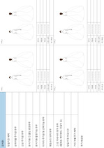
In D-FF in pic 1, module becomes activate when clock is positive edge or reset
button is pushed. In that case, D-FF delivers input value directly to output. 10-bit shift register was created with 10 D-FF. In pic 2 shift_register module by linking the results of the previous D-FF to the input of the next D-FF and receiving the first input with i_val, the input is shifted until it reaches 10th D-FF. Since reset button and clk is linked every D-FF
참고 자료
Yonsei univ. Electrical Electronic Engineering - Week 4 Lecture
Charles H. Roth, Jr.& Larry L Kinney. (2013). Fundamentals of Logic Design.
Cengage Learning